Products and services

We Specialise In

Being a one-stop supplier to our customers with our taping solutions (QFN Tape, Die Attach Film, Mold Release Film, Wafer Dicing Tape and EMI Carrier Tape) as well as our customised Paper Leadframes in order to exceed their expectations in cost-saving, problem-solving as well as process improvement.

QFN Tape

Our QFN Tape is highly heat-resistant and is adhered on the lead frame at the back of a semiconductor package to prevent EMC molding leakage. Even after the tape is removed, no adhesive residue remains. There is also no flash burr during EMC molding processing, little warpage of the lead frame even at high temperatures and excellent adhesive property with wires.

Our QFN Tape is suitable for applications in micro lead frames (MLF) as well as QFN/QFD packages.

QFN Packaging Process

Die Attach Film (DAF)

For our Die Attach Films (DAF), besides the standard Die-to-Die and Die-to-Substrate applications for multi-level Stacked Die Packages (SD Cards, u-SD Card, DDP, QDP, ODP, MCP, etc. ), our products are qualified for Die-to-Glass and Die-to-Ceramic applications in the Fingerprint Sensor (FPS) industries.

Compared to epoxy glue, they provide higher precision at a lower cost.

Our new single-layer PI-DAF

Our new double-layer PI-DAF

We are also the major provider of adhesive solutions for Fingerprint Cards AB, the world-leading Swedish biometric company which holds a large market share of the global smartphone and fingerprint sensing sector. Our DAF can certainly meet your FPS packaging requirements.

Our DAF has excellent workability (no burr), is highly reliable (MRL 2) and has a long dwell time even at high temperatures (150/2hr). We have the filler, no-filler, pre-cut and non-pre-cut types.

We also have Die Attach Films (DAF) for Film Over Die (FOD) applications, with an optimum design for blade and DBG processes in die separation and die pitching. It has good expansion as well as excellent embedding and filet control, which enable easy pick up. Our engineers use high-purity epoxy / hardener (CL<50ppm) to achieve HAST (110°C at 85%RH) after 320 hours. Corrosion is also prevented through the capturing of CL ions by ICA. There are no distortions or voids.

Mold Release Film

Our Mold Release Film is designed for use in the epoxy molding process which aims to protect semiconductor chips from the external environment with the epoxy molding compound (EMC). The Mold Release Film prevents the invasion of EMC during EMC injection. It can be used in various applications, such as in QFN Packages, Fan-Out Packaging, and more.

Properties of our Mold Release Films

No wrinkling of the film when mounted on to the mold.

No EMC leaks on the opposite sides of the package.

No deformation of the package during de-taping.

No contamination of acrylic adhesive layer on the backside surface of the package after detaping.

The Molding Process

EMI Carrier Tape

EMI shielding protects electrical circuits from disturbance by electromagnetic induction or radiation emitted by an external source. Our EMI Carrier Tape protects the bottom of your package during the EMI spraying or sputtering process. ​It is used in a variety of applications -- communication and RF devices, memory chips such as Nand Flash, as well as in sensors.

Properties of our EMI Carrier Tape

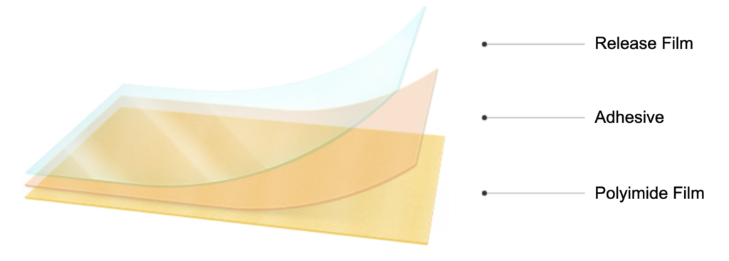
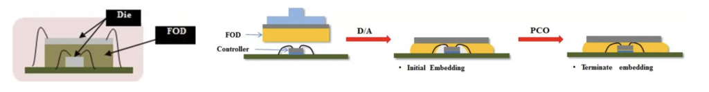
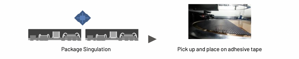
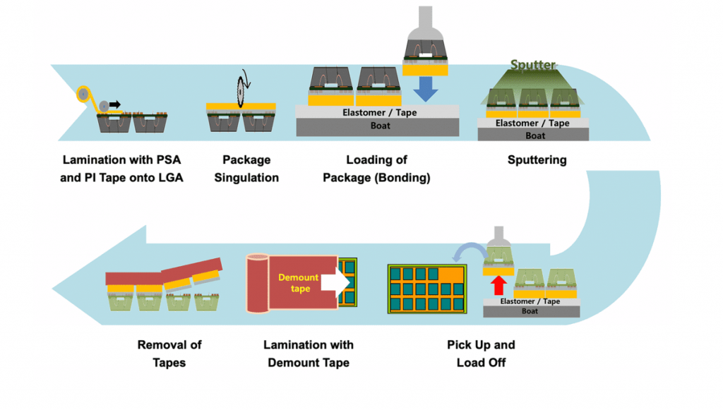
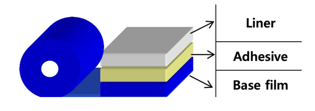
No contamination of the backside surface of the package by the silicone adhesive layer after detaping.

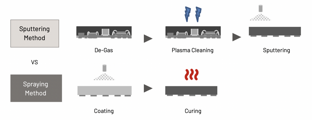
Low contamination of silicone by outgas during the EMI process.

Low contamination of the backside surface of the package caused by sputter material.

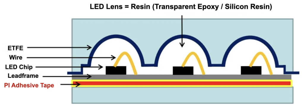
No overflowing of silicone resin at the sides of the package.

General Process for EMI Shielding

1st Step

SKYMART Technologies

For building a barrier between devices. Skip this process if unnecessary.

2nd Step

SKYMART Technologies

3rd Step

Although the spraying method is competitive in terms of cost, market players are preferring the sputtering method.

Process for EMI Shielding - Attachment of Tape

Process for EMI Shielding - LGA

Taping Method

SKYMART Technologies

Process for EMI Shielding - LGA & BGA

Taping Method for Laser Cutting

Process for EMI Shielding - LGA & BGA

Taping Method for Dipping (Non UV)

Process for EMI Shielding - BGA

Taping Method for Ball Dipping (UV)

Wafer Dicing Tape

Our Wafer Dicing Tape is designed for blade and SDBG processes. There is no burr, good die pitch, easy pick up, excellent chipping performance, stable adhesive strength after UV irradiation during the in--line process, and it leaves no adhesive residue on the wafer.

Paper Leadframes

We capitalise on our core competencies in mold design and leadframe stamping to produce paper leadframes for applications beyond mold cleaning.

We possess in-depth technical knowledge on the design and application of paper leadframes. Our engineers patiently optimise the size, thickness and cut of the design to achieve the best results and returns. Our custom designs help our customers get to the next level in their use of paper leadframes in their assembly processes.

We serve the largest US and European corporations and are the major supplier to Russia. Our factory locations in Singapore and South Korea will bring you the greatest value in cost, quality and service.

We offer paper lead frames with 3-4 layers, paper leadframes that are lint-free, as well as paper leadframes that can withstand high temperatures of 360° Celsius. We also manufacture paper substrate and epoxy lead frames.

Front: SKYMART Paper Leadframe, Back: Another supplier (after 30 seconds); gaps in capability and performance due to the selection of material as well as the design.

Samples of past designs we have customised for our esteemed clients.

Taping Solutions

We supply single and double-sided adhesive tapes used in the semi-conductor assembly process for attaching lead frames to chips or for bonding metal circuits. These tapes are produced under high-degree cleanroom conditions comparable to those of semiconductor assembly lines.